Exploring Maximum Power Transfer with 3D Plots in Matlab
May 13, 2015 Leave a comment
I recently took a course in circuit analysis where we learned the maximum power transfer theorem. While there are many plots of the power transfer in the purely resistive case, I did not see any for the case where the source and loads are impedances (with both resistance and reactance). I played around with 3D plots to get a better understanding of power transfer and to practice using Matlab. Here is a write-up of what I did.
Introduction
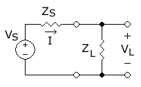
We will analyze the following circuit:
Image: “Source and load circuit Z“. Licensed under CC BY-SA 3.0 via Wikimedia Commons.
The relevant elements are as follows:
is the voltage source, which we assume to be a steady-state sinusoidal source.
is the source or internal impedance (with resistance
and reactance
).
is the load impedance (with resistance
and reactance
).
The idea is to find the amount of power transferred to the load by the voltage source given a fixed source impedance. We are particularly interested in finding the load impedance that will give us the maximum power transfer to the load. There are many references that discuss these concepts, so I will not go into more detail here. I will note however that there is an interesting article “Non-Calculus Derivation of the Maximum Power Transfer Theorem” by Dr. Kenneth V. Cartwright which discusses the theory in a non-traditional manner.
I will show the equations, but will not derive them – I will use the same notation and form as found in the “Maximum power transfer theorem” Wikipedia article. I will include short Matlab code blocks throughout this document. These are meant to be run in order (in other words, each code snippet will depend on variables or plots from previous snippets). I am no Matlab expert, so I am sure there are better ways to write and present the code. For variables, I use the following convention: scalar constants are designated with lower case letters, whereas vectors and matrices are designated with upper case letters. For simplicity, I use the value 1 for all constants. To get the most detail from the plots I include, you will need to click on the images.
Power Transfer with Pure Resistance
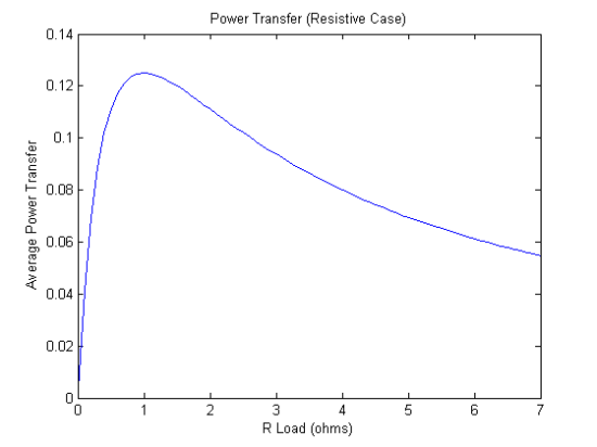
For the purely resistive case (), the average load power as a function of load resistance (we assume the source voltage and load resistance are constants) is:
The plot of this power function is found in many places. We can plot it ourselves as follows:
vs = 1;        % Source voltage is normalized to 1V
rs = 1;        % Source resistance is normalized to 1 ohm

RL = 0:0.1:7;  % Use load resistance in the range (0,5) ohms

% Calculate power
P = 0.5 * (vs.^2 .* RL) ./ ((rs + RL).^2);

% Plot the power
figure;
plot(RL,P);
title('Power Transfer (Resistive Case)');
xlabel('R Load (ohms)');
ylabel('Average Power Transfer');
As can be confirmed by the graph, maximum power transfer occurs at where
Power Transfer with Impedance
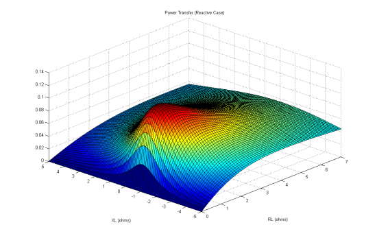
The load power as a function of load impedance (as before we assume the source voltage and load impedance are constants) is:
We can plot this function as follows:
xs = 1;        % Source impedance is normalized to 1 ohm

XL = -5:0.1:5; % Use load reactance in the range (-5,5) ohms

% Build a mesh grid for the 3D plot
[RL_mesh,XL_mesh] = meshgrid(RL, XL);

% Calculate power
P = 0.5 * (vs.^2 .* RL_mesh) ./ ((rs + RL_mesh).^2 + (xs + XL_mesh).^2 );

% Plot the power
figure;
surf(RL_mesh, XL_mesh, P);
title('Power Transfer (Reactive Case)');
xlabel('RL (ohms)');
ylabel('XL (ohms)');
Lines of Maximum Power Transfer
For a given we can find the
that gives the maximum power by solving the equation
to get:
Note that the impedance turns out to be independent of . We can plot a line to follow this maximum power:
% Calculate reactance where power is maximum for each resistance (note it is constant)
XLMAX = -xs * ones(size(RL));

% Calculate maximum power along the line
PMAX = 0.5 .* (vs.^2 .* RL) ./ ((rs + RL).^2 + (xs + XLMAX).^2 );

% Plot the line on top of the existing surface
hold on;
plot3(RL, XLMAX, PMAX,'LineWidth',2,'Color',[0 0 0]);
Likewise, for a given we can find the
that gives the maximum power by solving the equation
to get:
We can plot a line to follow this maximum power as well:
% Calculate resistance where power is maximum for each reactance
RLMAX = sqrt(rs^2 + (XL + xs).^2);

% Calculate maximum power along the line
PMAX= 0.5 .* (rs.^2 .* RLMAX) ./ ((rs + RLMAX).^2 + (xs + XL).^2 );

% Plot the line on top of the existing surface
hold on;
plot3(RLMAX, XL, PMAX,'LineWidth',2,'Color',[0 0 0]);
Maximum power occurs where the lines intersect. As can be confirmed on the graph, this occurs when the source and load impedances are complex conjugates of eachother:
As before the maximum power is .
Efficiency
The efficiency (power dissipated in the load versus total power dissipated) is a function of resistance only:
In the plots so far, the surface is colored automatically to match the magnitude of the power (blue indicates a smaller magnitude and red indicates a larger magnitude). We can also specify our own color scheme. For example we could color the surface to indicate the degree of efficiency:
% Calculate efficiency
EFF = RL_mesh ./ (rs + RL_mesh);

% Plot a new graph which indicates efficiency using color
figure;
surf(RL_mesh , XL_mesh, P, EFF);
title('Power Transfer (with Efficiency)');
xlabel('RL (ohms)');
ylabel('XL (ohms)');
Note that the numbers along the vertical axis of the graph still indicate power magnitude – efficiency is only indicated by color. As expected, the efficiency increases asymptotically to 100% as load resistance increases (dark blue indicates 0% and dark red indicates close to 100%).


